TSMC breaks ground on more advanced packaging fabs in Chiayi
The business move
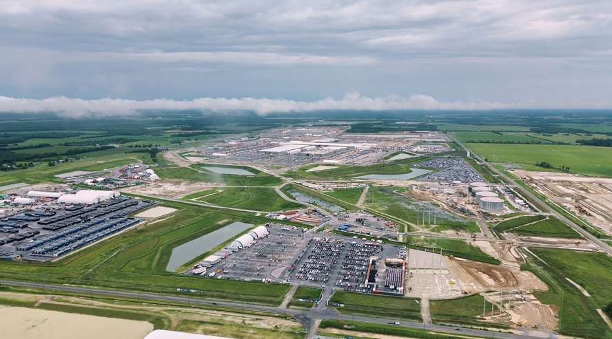
TSMC announced it will expand its advanced packaging capacity with new fabs in the second phase of Taiwan’s Chiayi Science Park. This move aims to relieve bottlenecks in chip packaging, a critical step for high-performance AI hardware. The announcement came from Taiwan’s National Science and Technology Council minister Wu Cheng-wen at a recent groundbreaking ceremony.
Why it matters
Packaging is a key choke point in the AI chip supply chain. It happens after wafer fabrication and before chips hit the market. As AI workloads demand tighter memory and faster interconnects, packaging sophistication becomes essential. Nvidia’s multi-year deal for HBM4 memory with SK Hynix exposed how constrained advanced packaging capacity can slow product availability. TSMC’s expansion signals efforts to ease this pressure and improve delivery timelines for AI accelerators and other advanced semiconductors.
Who gains and who gets squeezed
Chip designers and AI hardware providers stand to benefit from increased packaging capacity. Larger, more complex packages with multiple dies and advanced memory stacks become easier and cheaper to produce. Taiwan’s semiconductor ecosystem tightens its grip on the high-value packaging step, which could squeeze competitors reliant on external or less advanced services. Memory suppliers like SK Hynix may find some relief in the supply crunch, but overall demand and shortages could keep costs and lead times elevated across the board.
What to watch next
Monitor how quickly TSMC ramps the new packaging fabs and whether this expansion measurably reduces wait times for AI chip assembly. Also watch if other foundries or packaging specialists speed up investments or strike partnerships to keep pace. Changes here affect not just hardware makers but cloud providers and AI startups dependent on cutting-edge silicon getting to market on schedule.
AI Quick Briefs Editorial Desk